Project RAM.Bo32
A RAM Add-On Board for the Motorola 68HC912B32 EVB
Who needs RAM on the B32 EVB?
The Motorola B32EVB itself is a real nice evaluation and development board, but it only comes with the internal 32KB Flash Memory of the 912B32 MCU. This internal Flash is only guaranteed to be re-programmable 100 times, if you take the specs seriously. That is, if you debug your application and try out a large number of program versions, you *could* exceed the Flash Memory life time very soon.
Another reason is, that the entire Flash array is occupied by the D-Bug12 monitor. If you erase the Flash and load your own program, you can not use the monitor anymore to debug your application.
In addition, loading S-Records into RAM is much easier than programming the Flash Memory, which requires a lot of preparation and time. So why not adding an external RAM device via the bus interface of the 912B32? That would be very helpful while developing an application...
That was the point where I started looking at timing specs in the "Electrical Characteristics". Very soon it became obvious: It's not a simple task to find a reliable solution. The bus timing is tight and the specs are rather confusing. Finally, I decided to create a working example.
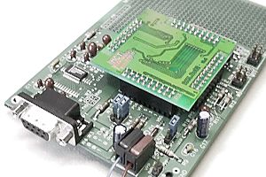
That was the starting point for RAM.Bo32: A RAM Board for the 912B32 providing such a memory expansion. It's a small PCB suitable to simply plug it onto the four header connectors on the 912B32 EVB from Motorola. On the add-on board there is a 64K x 16 Memory Chip (15ns), together with the desired glue logic. The memory space of the 912B32 is only 64KB, so there are two independent 64KB spaces (which can be toggled using port pin PS3 of the MCU).
Schematic Diagram
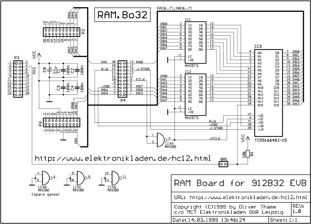
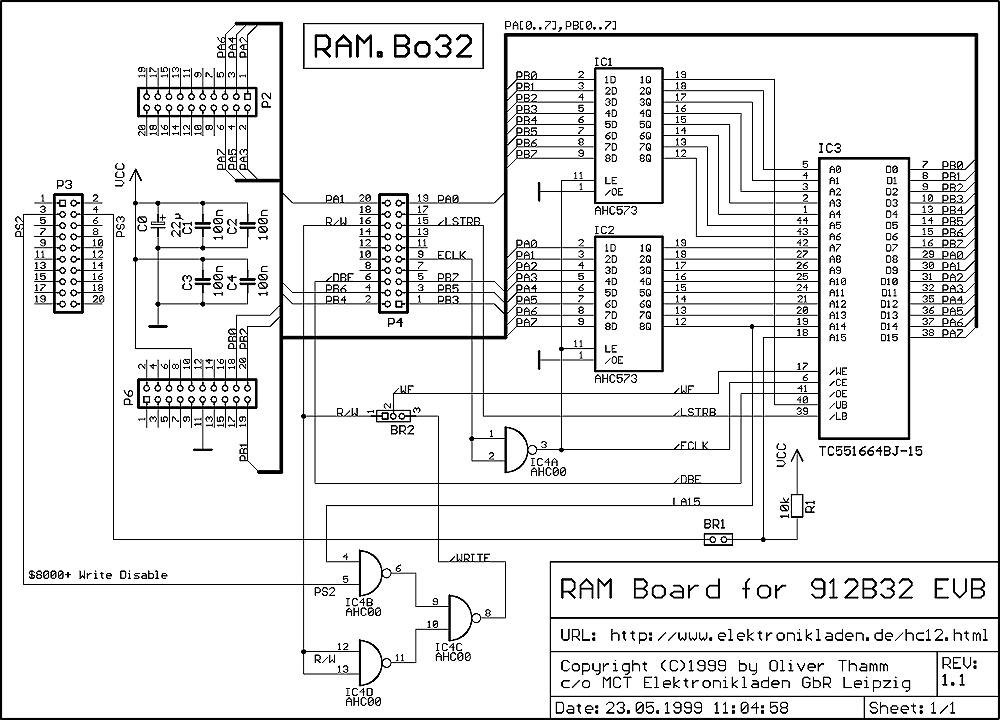
Main component of the Add-On Board is a 16 bit wide Fast Static RAM from Toshiba, accompanied by some AHC Logic ICs from Texas Instruments. The schematic diagram below shows all the details you might wish to know about RAM.Bo32 (click on the picture to display a larger version).
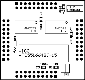
The place plan
The place plan on the right shows, how the board is operated (mechanically): just plug it onto the four header connectors of the B32 EVB. The dimensions of the board are approx. 1.8" by 2" - just the size given by the header connectors. I think that is the best solution, because one can reach the reset button, jumpers and connectors on the EVB - the add-on RAM board should not hide something on the base board. On the other hand, it would be nice to have (the same) connectors on the upper level (that is, on the RAM board), even if it will consume more space. Pro and cons...
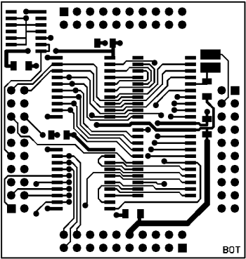
The PCB Layout
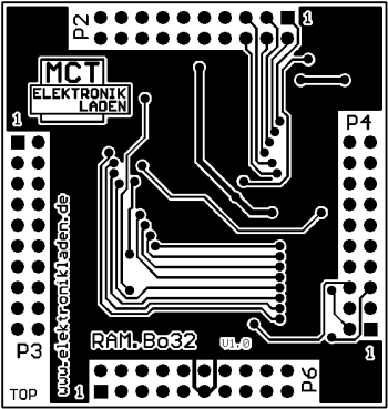
Here comes the layout for both the top and the bottom side of the PCB. Please note, that all components are SMD (surface mounted) and they are all mounted on the bottom side!
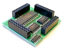
A first prototype!
The prototype PCBs arrived from the PCB manufacturer within two weeks. After soldering the SMD components and the header connectors on both the RAM.Bo32 and the EVB, it got thrilling (as everytime when power is applied for the first time). But everything turned out to work fine. At least, no clouds :-)
To get access to the RAM only one thing remained to be done: to enable the external bus interface by setting the MODE register. This sounds simple? Well, it isn't! Since the D-Bug12 monitor accesses the MODE register during start-up, it is not possible to change it again later - in Normal Mode it can only be written once. That means, it was necessary to patch the monitor code.
The soft(ware) side
The basis for the following changes was D-Bug12 V2.02 for the B32 EVB, which seems to be the latest firmware version available from the Web. It contains an initialization sequence, which is documented in the B32 EVB manual (the listing shown here was adapted to be assembled using the Imagecraft ICC12 compiler). At least one patch is needed (marked red) to switch from Normal Singlechip Mode to Normal Expanded Wide Mode:
*******************************************************************************
; INITIALIZATION
; The code in this section is initialization for the monitor on the EVB12B32
;*******************************************************************************

__MonStartup:
            lds #STACKTOP               ; initialize monitor stack pointer
;
;   Disable the COP watchdog by CR2:CR1:CR0 = 0:0:0
;   COPCTL = $07 when reset in normal modes
;   FCME and CRx bits are write once in normal modes
;   COPCTL [ CME :FCME : FCM : FCOP ! DISR : CR2 : CR1 : CR0 ] $--16
;
            clr COPCTL                  ; disable watchdog
;
;   Clear all monitor RAM to start from a known state
;
            ldx #MonRAMStart
ClrRAM:     clr 1,x+                    ; clear one and inc pointer
            cpx #MonRAMStart+MonRAMSize
            bne ClrRAM                  ; loop till RAM clear

;   Enable pipe signals, E, low strobe and read/write in port E
;   PIPOE, NECLK, LSTRE and RDWE are write once in normal modes
;   PEAR [ARSIE :CDLTE :PIPOE :NECLK !LSTRE : RDWE : 0 : 0 ] $--0A
;
            ldaa #$2c                   ; prevent later protection lock
            staa *PEAR                  ; PROTLK is write-once

;   Without changing modes, enable internal visibility
;   MODE [SMODN : MODB : MODA : ESTR ! IVIS : 0 : EMD : EME ] $--0B
;
            bset *MODE,$08              ; set IVIS
;
;           bset *MODE,$68              ; set IVIS + switch to Expanded Mode

;   Enable EEPROM so monitor can program/erase bytes
;   EEMCR [ 1 : 1 : 1 : 1 ! 1 : 1 :PROTLK: EERC ] $--F0
;   BPROT [ 1 :BPROT6:BPROT5:BPROT4!BPROT3:BPROT2:BPROT1:BPROT0] $--F1
;
            ldaa #$fc                   ; prevent later protection lock
            staa *EEMCR                 ; PROTLK is write-once
            clr BPROT                   ; allow EE program and erase
;
;   Disable writing to the on-chip Flash EEPROM
;   FEELCK [ 0 : 0 : 0 : 0 : 0 : 0 : 0 : LOCK] $--F4
;
            ldaa #$01                   ; write a 1 to the Flash LOCK bit to
                                        ; disable accidential reprogramming of
            staa *FEELCK                ; the flash memory (where we're located)
;
            ldd EEBase                  ; get the user supplied base address of the
                                        ; on-chip EEPROM

            oraa #1                     ; make sure that the EEON bit remains set.
            staa *INITEE                ; re-map the on-chip EEPROM.
;
            ldd IOBase                  ; get the user supplied base address of the
                                        ; on-chip I/O registers
            staa *INITRG                ; re-map the on-chip registers.
            ldx #_UserFnTable           ; point to the table of user accessible
                                        ;routines.
            jmp [0,x]                   ; the first entry is a pointer to main.
                                        ; GO.........
The byte to change ($68 instead of $08) is located at $F716 and can be patched manually in the S-Record file using a text editor.
Now you can set jumpers W3 and W4 to position "1" to establish download mode, apply programming power to the EVB, (E)rase the Flash array and (P)rogram the patched version. Voila! Enjoy downloading your code straight into kilobytes of RAM!
Even more fun!
Did you ever ask yourself how to modify the interrupt vectors in order to implement an interrupt handler in your application code? Hm... they are located in the Flash area, so it's not possible to modify them "on the fly". It's not even possible to re-program them (w/o a BDM tool), because they are in the protected boot block!
Okay, D-Bug12 contains some means to set up a sort of interrupt pseudo vectors, but they are still in Flash - so you have to go through that boring erase-the-flash-and-program-it-with-your-code procedure again and again. Wouldn't it be great to just download interrupt vectors together with the rest of the application? No problem, if Flash would be RAM...
Indeed, it's not a problem! Just modify the D-Bug12 startup routine in the following way:
- Establish Normal Expanded Mode
- Copy Flash contents to the external RAM
- Remove the Flash array from the MCU's memory map
- Continue execution - in RAM!
If you accidental overwrite something important - no problem, just press the reset button to reload the D-Bug12 image from Flash!
So far, so good. But there is one point (No.2!) which causes a serious problem. Copy Flash contents to RAM would be simple, if one could switch the Flash on and off several times. The strategy simply would be, to read a byte from Flash, disable the Flash, store the byte in RAM (using the same address) and then enable the Flash again, reading the next byte and so on. But the responsible register (MISC) can only be written once if the MCU is in a Normal Operating Mode.
Finally, Mark Schultz (thanks Mark!!) made this contribution to the project: He had the brilliant idea to use a side effect of the HC12 bus interface. If you have ever worked with the HC11 you'll know the fact, that all internal bus activities are visible on the external bus as well. If the CPU reads a byte, the internal bus will be accessed, so no matter what happens externally. If a write occures, both the internal and the external memory will (attempted to) be written. If the IVIS bit in the MODE register of the HC12 is set, internal bus actions are visible in the same way. That's the way out! The routine to copy the monitor just consists of a loop which reads from the Flash array and immediately writes the value back to the address. This does not effect the Flash, but the RAM outside!
Look at the details: The modified D-Bug12 startup source and executable
Compatibility with the BC32 version:
Yes, RAM.Bo32 also fits on the Motorola BC32EVB! This Evaluation Board has a different layout (compared to the B32EVB), but the header connectors are at the same position with the same contacts. Here is a picture of this rare EVB containing a PC68HC912BC32 MCU. It seems that it comes from Scotland, not from the US.
All you need is speed!
Here comes a nice suggestion from Dan Miner. He demonstrates, how to efficiently use the HC12 instructions to improve copy speed in the startup code. Dan writes:
I just noticed your startup code. In the interest of learning together, I think I can speed it up and save a byte. Your code:
;   Copy Flash contents to RAM
;
            ldx  #$8000                 ; block start
_flash2ram: ldd  0,x                    ; read from Flash (internal)
            std  0,x                    ; write to RAM (external)
            inx
            inx
            bne  _flash2ram             ; loop if (X<=$FFFF)
;-------  Loop is 8 bytes, 10 cycles per word. ------
Note: My version is untested at the moment but is provided here for academic interest. My code:
            ldx	#$8000
_flash2ram:
            movew	0,x, 2,x+
            tbne	x, _flash2ram
;-------  Loop is 7 bytes, 8 cycles per word. ------
The Bus Timing
If you study the timing diagrams of the 912B(C)32 multiplexed bus (see Motorola document Electrical Characteristics), you still may have questions - to say it in a polite way. Most likely, you come accross the following questions:
- Will the addresses be valid *before* E-clock rises?
- Whats the behaviour of the /DBE signal?
- When does the MCU actually switch from address to data output (during a write operation)?
- How do the timing parameters of the real hardware (together with the Add-On Board) look like?
To gather some more information about all that timing stuff, I connected the relevant bus signals to a 1 GHz HP logic analyzer. The diagrams below show the results. PB0..2 are the lowest three bits of the multiplexed address/data bus. The measurements were made at room temperature on a B32EVB with a PC68HC912B32CFU8 (mask revision 2H91F) and the RAM.Bo32 Add-On Board (15ns Fast Static RAM).
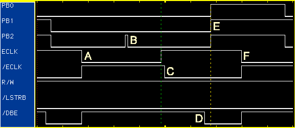
MCU reads $xxxF from address $xxx0 (Expanded Wide Mode, no stretches), Timing: 20ns/div
The bus cycle starts at mark A. After 35ns a spike at position B shows a bus activity, obiously the MCU establishes the adresses for this cycle. In other words: the addresses are valid more than 25ns before ECLK rises. That is approximately at the same time when R/W and /LSTRB changes (we don't have such a change here, but it's visible in the next diagram). The negated ECLK (4ns delayed by the AHC gate, see mark C) is used to latch the adresses using IC1 and IC2. It also provides the chip enable signal for RAM IC3. 33ns after ECLK got H, the MCU activates /DBE (mark D). 6ns later the Fast Static RAM drives the data bus (mark E). /DBE remains Low for another 23ns and gets inactive at the same time ECLK goes Low (mark F). An interesting detail: The /ECLK delay caused by the AHC gate with an H-L input is much smaller (1ns or below) than for the other edge (4ns).
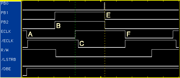
MCU writes $xxx0 to address $xxxE (Expanded Wide Mode, no stretches), Timing: 20ns/div
The second diagram shows a write cycle. Adresses become valid approx. at the same time as R/W goes Low (mark B). The time between ECLK rise and output of data by the MCU (mark E) is 39ns. This is exactly the same timing value, as found in the read diagram above! Seems that the RAM we've connected meets the HC12's desires pretty well...
One problem remains: What about the Read Data Setup Time which should be 30ns according to the Motorola specs? Is it important? I think, it is not. Let's simply assume, Motorola means it in the way "During a read cycle, the bus can be occupied by an external device (at least) 30ns before the falling edge of ECLK." Designing with the B(C)32 becomes so easy with this definition :-)
Spare Gates
Unused gates are a *nightmare* for every design engineer :-) and there are three of them in the schematic above. It was Dan Miner again, who sent me the following interesting suggestion:
I just thought of another POSSIBLY useful modification to your board. It only uses the 3 extra NAND gates that are already there and allows the upper half of the SRAM to be optionally write protected. This is where the FlashROM code gets copied to.
Definitions:
A15 = IC2 pin12 (and IC3 pin 19)
R/W = P4 pin 16
/WE = IC3 pin 17
WP  = P3 pin 3 = HC912 PS2 = Write Protect line
- Cut current connection between R/W and /WE.
- Cut all ground jumpers to unused inputs on IC4.
- Connect R/W to IC4D pin 12 and IC4D pin 13 (Create W/R)
- Connect A15 to IC4B pin 4
- Connect WP to IC4B pin 5
- Connect IC4B pin 6 to IC4C pin 9
- Connect IC4D pin 11 (= W/R) to IC4C pin 10
- Connect IC4C pin 8 to IC3 pin 17 (= /WE)
Truth table:
PS2  A15  R/W  /WE
 0    0    0    0
 0    0    1    1
 0    1    0    0
 0    1    1    1
 1    0    0    0
 1    0    1    1
 1    1    0    1   *** When PS2=1 and A15=1, no write to SRAM!
 1    1    1    1
So your startup code now needs to:
- Make WP (SP2) an output and = 0
- Copy FlashROM to SRAM
- Set WP (SP2) = 1 (Write protects SRAM $8000 to $FFFF)
- Disable FlashROM
I'm thinking of protecting the code from a run-away program while it still has bugs in it. To make intentional changes to the code, just set WP=0, make changes, then return WP=1.
The best of both worlds: A code image that is read-only but easily modifiable when you want. (As often as you want!)
I very appreciate Dan's contribution and will modify the PCB accordingly!
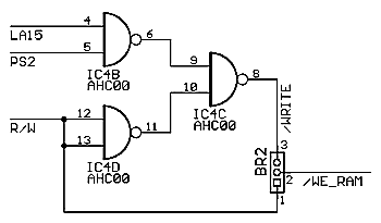
The schematic on the right summarizes the necessary changes. The solder bridge BR2 is used to select the method for generating the write enable signal for the RAM (just using MCU R/W or Dan's way).
The final cut: Version 1.1
The latest PCB version 1.1 now has the RAM Protect Option build-in (for a detailed description see above!).
Here comes the new schematic diagram:
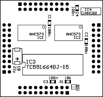
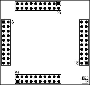
The two Silk Screen pictures show how the parts are placed on the PCB and where to find the solder bridges BR1 and BR2.
Left: bottom side = component side. Right: top side.
You will also need to download the included Rev.D patched D-Bug12 V2.02 S-Record file to the EVB. The patch establishes a modified Monitor Startup Code, which not only copies the Flash contents to RAM, but also toggles the Write Protect line (WP=PS2) as described above. The ZIPed file contains the source file, so you can check what exactly happens.
To load the new monitor version do the following:
- Set the jumpers W3 and W4 on the B32EVB both to "1" and reset the B32EVB
- Apply programming voltage (Not above 11.8V - check the data sheet of your MCU mask revision!!!) to W8 "VPP Input"
- Set W7 from VDD to VPP
- Erase the Flash array (the boot block will not be erased, anyway)
- Program the new S19 file
- Set W7 back to VDD, remove the programming voltage
- Set W3 and W4 both to "0" to establish EVB mode
- Reset the B32EVB and - nothing will happen if you forgot to plug in the RAM.Bo32 board...
Download Board & Schematic
I have decided to make the whole project freely available for non-commercial (read: non-profit) use, so enjoy it and download the Board and Schematic Files of the RAM.Bo32 V1.1 PCB.
The Ram.Bo32 PCB was designed with Eagle. This PCB was made with V3.5, but the new V4 should work fine, too.
That's all for now - Good luck!
About the Author, Copyright stuff
The RAM.Bo32 project is Copyright by
Oliver Thamm
Leipzig, Germany
Please send suggestions and inquiries concerning this page to ot hc12web.de
Deutsche Version: siehe Artikel in Design & Elektronik 7/99 RAM! Mehr RAM! (Online Version)
The original URL of this page is http://hc12web.de/rambo32/
Back to Oliver Thamm's HC12 Web
